In China, the local semiconductor industry is gradually promoting homegrown lithography tools following the specifications published by the central government of the Asian country, but analysts through the prism of skeptical perception assess the quality level of this movement forward, noting in an appropriate context that Beijing has yet to make a kind of breakthrough in progress to fully compete with the Dutch company ASML, which is the world’s leading manufacturer of equipment for making chips.
The Ministry of Industry and Information Technology of China, which is responsible for overseeing the development of the domestic sector of microcircuits production, released a list of new tools for the appropriate sphere of activity this month. The purpose of the relevant list as a matter of priority is to encourage local chip makers to use the mentioned tools.
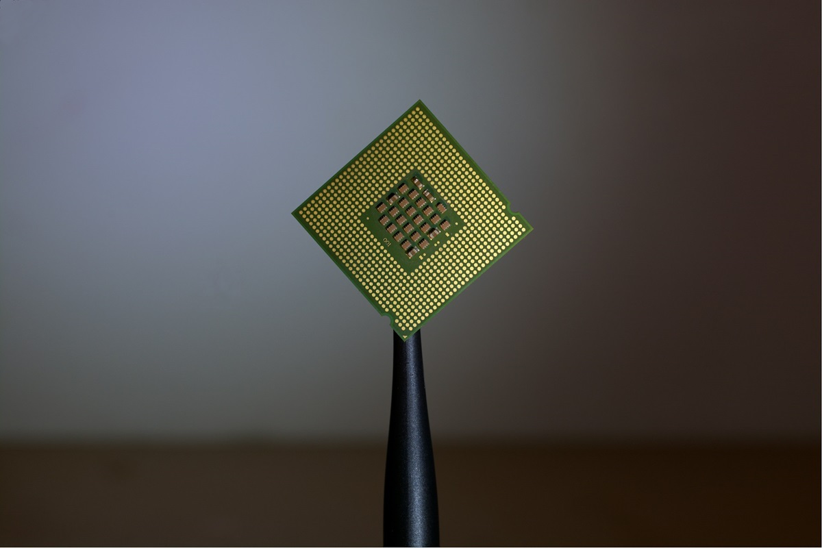
It is worth noting that Beijing’s moderate movement forward does not mean an absolute lack of progress and lack of any positive results. Despite skepticism, analysts and international media have nevertheless drawn attention to the mentioned list of tools that are used at various stages of the production process, including, among others, the manufacture of integrated circuits, mining, and metallurgy. Experts positively assessed the presence of two lithography scanners in this list. They described these tools as a sign of progress in the evolution of China’s semiconductor industry.
According to the information which is contained in a document published by the Ministry of Industry and Information Technology of an Asian country, one of the lithography scanners is equipped with a krypton-fluoride (KrF) light source with a 248-nanometer wavelength and an overlay accuracy below 25nm, which provides a resolution of 110 nm on 12-inch wafers. Another lithography scanner uses a more advanced argon fluoride (ArF) light source with a 193nm wavelength and an overlay accuracy below 8nm. In this case, a resolution of 65 nm is provided on 12-inch wafers.
It is worth noting that the Ministry of Industry and Information Technology of China has not released information about the manufacturers of the mentioned machines. It is also currently unknown how many wafers per hour these lithography scanners can produce. Besides, it’s worth noting that in the document published by the ministry, there is no information about the capabilities of machines for feature alignment. At the same time, it is this indicator that determines how advanced lithography scanners might be.
It is worth noting that at present, the chip manufacturing sector is what can be described as a battlefield within the framework of technological confrontation in the context of geopolitical tensions that show no signs of strengthening and no signal of an imminent end or at least a softening of the corresponding state of affairs. Microcircuits are now a critical commodity. This thesis is confirmed by the fact that chips are currently used in many industries and products that people interact with on a large scale daily. For example, microcircuits are already an element of car equipment and an important component of smartphones and personal computers. It is worth noting separately that chips are necessary for the development, training, and maintenance of the subsequent operation of artificial intelligence systems. At the same time, AI is actually the main technology of modernity. Artificial intelligence has the potential to become a new means of production that can transform many sectors of industry, in particular, and the economy as a whole. Also, an AI capable of generating information materials and even works of art can have a fundamental impact on the social environment, the cultural area, and the space of political processes. At the same time, the development of artificial intelligence is impossible without such a basic element as a chip in this case. The prospects for the future evolution of AI are impressive. Some experts predict that over time, artificial intelligence will surpass the capabilities of human consciousness in terms of cognitive abilities. For example, Elon Musk holds a similar point of view. The implementation of the mentioned scenario will mean the evolution of artificial intelligence to such a stage of existence as an autonomous form of mind capable of independent development and cognition of the world as the global matter of the being as a philosophical universal category at a level exceeding human abilities. Against the background of these prospects, it is obvious that the degree of access of a certain country to microcircuits or the condition of the homegrown semiconductor industry will determine its economic power and position in the international political arena.
The United States has imposed restrictions on the supply of advanced chips and equipment necessary for manufacturing products of the corresponding category to China. Since October last year, these restrictions have included clarification in the form of an allowable level of accuracy for systems using dedicated chuck overlay (DCO), a standard for measuring feature misalignment between two layers exposed by the same machine.
A more complex standard, called matched-machine overlay, checks for the alignment of patterns created using different machines. It is worth noting that modern fabrication plants often use different machines to print features on the same wafer. This solution is designed to make chips with billions of transistors.
Several anonymous analysts, while talking to media representatives, said that the new machines most likely refer to the DCO. In their opinion, this probably means a lack of ability to produce chips close to the 8nm level.
Any product smaller than 65 nm requires multiple patterning, however, the 8nm overlay accuracy might not be able to support any multiple patterning processes.
An ASML engineer, during a private conversation with media representatives, stated that there is often a ratio between dedicated chuck overlay and the on-product overlay in real manufacturing. According to the specialist, this is like building blocks one layer after another. The ASML engineer also noted that if the misalignment figure between layers is 8nm, it means the manufacturer can’t build a block with an accuracy smaller than 8nm.
The mentioned interlocutor of the media representatives stated that the best possible production nodes supported by the machine do not directly translate into the smallest feature achievable. In the relevant context, the ASML engineer noted that this largely depends on the technical knowledge of a foundry. The interviewee also stated that with the same tool, Taiwan Semiconductor Manufacturing Company can probably make 7nm-grade chips, while mainland China’s Semiconductor Manufacturing International Corporation can only make 16nm-grade chips. Speaking symbolically, the ASML engineer noted that lithography tools are like knives, but the taste of the dish ultimately depends largely on the chefs.
DCO is the most important yardstick for determining the capabilities of a scanner in real production through the use of technologies such as double and quadruple patterning.
A kind of fame for the esoteric standard was provided by the Commerce Department of the United States, which mentioned it in its updated export restrictions unveiled last year. At that time, the US banned the supply of machines with an alignment accuracy within 2.4 nm to China. This decision effectively deprived ASML of the opportunity to sell its 1980 and 1970 machines for immersion deep ultraviolet lithography to customers from an Asian country without a license.
The ASML 1980i model, which operates an ArF light source with a wavelength of 193 nm and can process 275 wafers per hour, has a DCO of less than 1.6 nm and a matched-machine overlay of 2.5nm for full wafer coverage. The ability to produce chips at 10 nm and below has made this model a sought-after equipment among foundries in China.
It is worth noting that the foundries of the Asian country stockpile equipment produced by ASML. The intensity of the relevant actions increased against the background of expectations of a tightening of the export control regime by the United States. These decisions of Washington were supported by some of its allies, including Amsterdam. It is worth mentioning that in January, ASML stated that it had received an order from the Dutch government to stop the supply of some of its products to China.